This chapter presented an in-depth investigation of the characteristics of amplifiers implemented using single transistors. - Of the three available device terminals of the BJT, only the base and emitter are useful as signal input terminals, whereas the collector and emitter are acceptable as output terminals. For the FET, the source and gate are useful as signal input terminals, and the drain and source are acceptable as output terminals. The collector and drain are not used as input terminals, and the base and gate are not used as output terminals.
- There are three basic classifications of amplifiers: inverting amplifiers -- the common- emitter and common-source amplifiers; followers -- the common-collector and common-drain amplifiers (also known as emitter followers or source followers); and thenoninverting amplifiers -- common-base and common-gate amplifiers.
- Detailed analyses of these three amplifier classes were performed using the small-signal models for the transistors. These analyses produced expressions for the voltage gain,current gain, input resistance, output resistance, and input signal range, which are summarized in a group of important tables:
| Table 14.1 C-E/C-S Amplifier Summary | page 988 | | Table 14.3 C-C/C-D Amplifier Summary | page 998 | | Table 14.5 C-B/C-G Amplifier Summary | page 1006 | | Table 14.7 Single-Transistor Bipolar Amplifiers | page 1008 | | Table 14.9 Single-Transistor FET Amplifiers | page 1011 | | Table 14.16 Four-Terminal MOSFET Amplifier Summary | page 1048 |
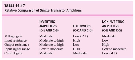
The results summarized in these tables form the basic toolkit of the analog circuit designer. A thorough understanding of these results is a prerequisite for design and for the analysis of more complex analog circuits. - Inverting amplifiers (C-E and C-S amplifiers) can provide significant voltage and current gain as well as high input and output resistance. If a resistor is included in the emitter or source of the transistor, the voltage gain is reduced but can be made relatively independent of the individual transistor characteristics. This reduction in gain is traded for increases in input resistance, output resistance, and input signal range. Because of its higher transconductance, the BJT more easily achieves high values of voltage gain than the FET, whereas the infinite input resistance of the FET gives it the advantage in achieving high input resistance amplifiers. The FET also typically has a larger input signal range than the BJT.
- Emitter and source followers (C-C and C-D amplifiers) provide a voltage gain of approximately 1, high input resistance, and low output resistance. The followers provide moderate levels of current gain and achieve the highest input signal range. These C-Cand C-D amplifiers are the single-transistor equivalents of the voltage-follower operational-amplifier configuration introduced in Chapter 11.
 <a onClick="window.open('/olcweb/cgi/pluginpop.cgi?it=jpg::::/sites/dl/free/0072320990/81006/table14_17.jpg','popWin', 'width=592,height=314,resizable,scrollbars');" href="#"><img valign="absmiddle" height="16" width="16" border="0" src="/olcweb/styles/shared/linkicons/image.gif"> (26.0K)</a> <a onClick="window.open('/olcweb/cgi/pluginpop.cgi?it=jpg::::/sites/dl/free/0072320990/81006/table14_17.jpg','popWin', 'width=592,height=314,resizable,scrollbars');" href="#"><img valign="absmiddle" height="16" width="16" border="0" src="/olcweb/styles/shared/linkicons/image.gif"> (26.0K)</a>
- The noninverting amplifiers (C-B and C-G amplifiers) provide voltage gain, signal range, and output resistances very similar to those of the inverting amplifiers but have relatively low input resistance and a current gain of less than one.
- All the amplifier classes provide at least moderate levels of either voltage gain or current gain (or both) and are therefore capable of providing significant power gain with proper design.
- Table 14.17 presents a relative comparison of these three amplifier classes.
- Design examples were presented for amplifiers using the inverting, noninverting, and follower configurations, and an example using Monte Carlo analysis to evaluate the effects of element tolerances on circuit performance was also given.
- The values of coupling and bypass capacitors can be chosen by setting the reactance of the capacitors to be much smaller than the Théeven in equivalent resistance that appears at the capacitor terminals. The reactance is calculated at the lowest frequency in the midband region of the amplifier's frequency response. The lower cutoff frequency fL is determined by the frequency at which the capacitive reactance equals the equivalent resistance at the capacitor terminals. In the amplifiers in this chapter, there are two or three poles that interact to set fL, and bandwidth shrinkage moves the cutoff frequency above that set by each individual capacitor acting alone.
- The analysis of the three basic amplifier configurations was extended to include the effects of field-effect transistors operating as four-terminal devices; Table 14.16 summarized the results of these analyses. In general, body effect, characterized by the parameter η, tends to improve the small-signal characteristics of amplifiers. However, we will later see that body effect degrades the dc biasing characteristics of some amplifiers.
|